In the semiconductor world, integration is omnipresent, driven by Moore’s Law. Integration reduces power and cost while increasing performance. The latest realization of this trend is the System-on-a-Chip (SoC) approach pervasive among PCs, tablets, and smartphones. And the latest SoC is Haswell.
Haswell is the first new family of SoCs from Intel to target the 22nm FinFET process, which uses a non-planar transistor that wraps around the gate on three sides. While Ivy Bridge was the first family of 22nm products, it was not fully optimized for the 22nm process. The CPU was a shrink of the 32nm Sandy Bridge rather than a new design.
The Haswell family encompasses a new CPU core, a new GPU, and numerous system-level changes. More importantly, it marks the beginning of Intel’s more unified approach to SoCs. The Haswell family is really a set of building blocks that architects will assemble for specific markets. The Haswell CPU core is a step forward in performance (as is to be expected from Intel) but more importantly, it is a huge step down in power. This SoC should be viable for high-end tablets. Variants of Haswell are aimed as low as 10W, and future improvements may reduce this further. Intel’s 22nm FinFET node is necessary to achieve this wider range, but it’s not sufficient. Haswell’s architecture fully exploits the benefits of the new process technology in a way that Ivy Bridge never did. It ultimately yields higher performance and lower power, which will translate into PCs and tablets that run faster with a longer battery life.
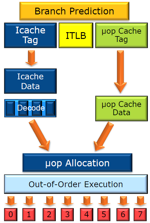
At the instruction set level, the Haswell core supports four extensions that profoundly transform the x86 ISA. AVX2 widens integer SIMD (Single Instruction Multiple Data, a form of vectors) to 256-bit vectors, and that adds a gather instruction for irregular memory access. The fused multiply-add (FMA) instructions improve performance for floating point (FP) workloads. For cryptography, networking, and certain search operations, there are new bit manipulation instructions. Lastly, Haswell is the first widely available product with transaction memory through the TSX extension. TSX is an incredibly powerful model for multi-threaded programming that improves performance and efficiency of software by better utilizing the underlying multicore hardware. Microarchitecturally, the Haswell core achieves even higher performance than Sandy Bridge. The improvements are mainly in the out-of-order execution—especially the memory hierarchy. It all strengthens Haswell’s case to be the basis of Intel’s upcoming generation of products in everything from tablets to servers.


 Loading comments...