As noted recently by Chipworks, Apple is now shipping some iPad 2 models (and all third-generation Apple TV devices) with a 32nm A5 processor built on Samsung’s power-efficient “high-dielectric metal gate” (HK+MG) process. These products give Apple a relatively low-volume test bed to ensure its architecture works well with the process, and extensive testing by AnandTech shows that the 32nm process offers significant power savings over the older 45nm process used for processors in other iOS devices.
Apple’s A4, A5, and A5X processors, used in the most recent iPhone, iPad, and iPod touch models, are built using the 45nm process. Effectively, 45nm is the absolute smallest size that can be used to create a transistor or other circuit element on a chip using a 45nm process. This also affects the minimum distance between elements as well.
Moving to a smaller process, in this case 32nm, typically reduces the size of the circuit elements. This has two benefits: less power is needed to drive the transistors and other elements, and a particular chip design will take up less space. So a 32nm A5 is about 40 percent smaller than the 45nm A5.
It also uses less power to operate, but shrinking transistors beyond a certain size increases what’s known as leakage current. What happens is that the microscopic bits of a transistor get so close together that some current can “leak” through it even when the transistor is switched to “off.”
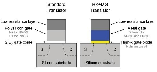
To counteract that leakage current, Samsung uses a combination of a high-dielectric material and metal to create a more efficient gate. It’s more complicated to manufacture compared to previous gate compositions, which is why Samsung hasn’t used it until now. (By comparison, AnandTech said that Intel transitioned to HK-MG nearly five years ago.)

 Loading comments...